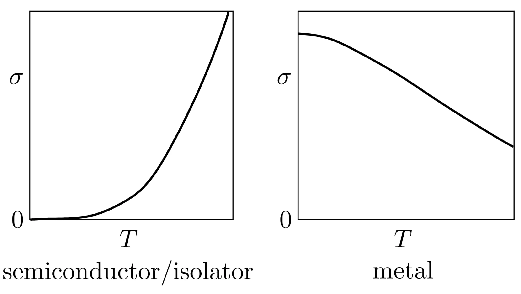
The technological relevance of semiconductors can hardly be overstated. In this chapter, we review some of their basic properties. Regarding the electric conductivity, semiconductors are placed in between metals and insulators. Normal metals are good conductors at all temperatures, and the conductivity usually increases with decreasing temperature. On the other hand, for semiconductors and insulators the conductivity decreases upon cooling.
We will see that the conductivity may be written in the Drude form as
where is the density of mobile electrons, is the average time between two scattering events of the electrons (transport life time of electrons) and and are the electronic mass and charge, respectively. In metals, is essentially independent of temperature, whereas the scattering time decreases with increasing temperature. Thus, determines mainly the temperature dependence of the conductivity in metals. On the other hand, insulators and semiconductors have no mobile charges at . At finite temperature, charges are induced by thermal excitations which have to overcome the band gap between the valence and the conduction band, yielding
where and the electron density in the material is typically . Actually, one has to count both the excited electrons in the conduction band and the resulting holes in the valence band, as both contribute to the current,
where + and - stand for holes and electrons, respectively, and holds for thermal excitation. Note that, in general, the effective masses and scattering times are not the same for the valence and conduction bands.
For insulators, the energy gap is huge, for example, for diamond. Consequently, the charge carrier density at room temperature is around . For a higher charge carrier density , smaller gaps are necessary. Materials with a band gap in this regime are not fully isolating and, therefore, are termed semiconductors. However, the carrier densities of both insulators and semiconductors are dwarfed by the electron density in metals contributing to current transport (). Adding a small amount of impurities in semiconductors, a process called doping with acceptors or donors, their conductivity can be engineered in various ways, rendering them useful as components in innumerable applications.
2.1 The Band Structure of the Elements in Group IV
2.1.1 Crystal and Band Structure
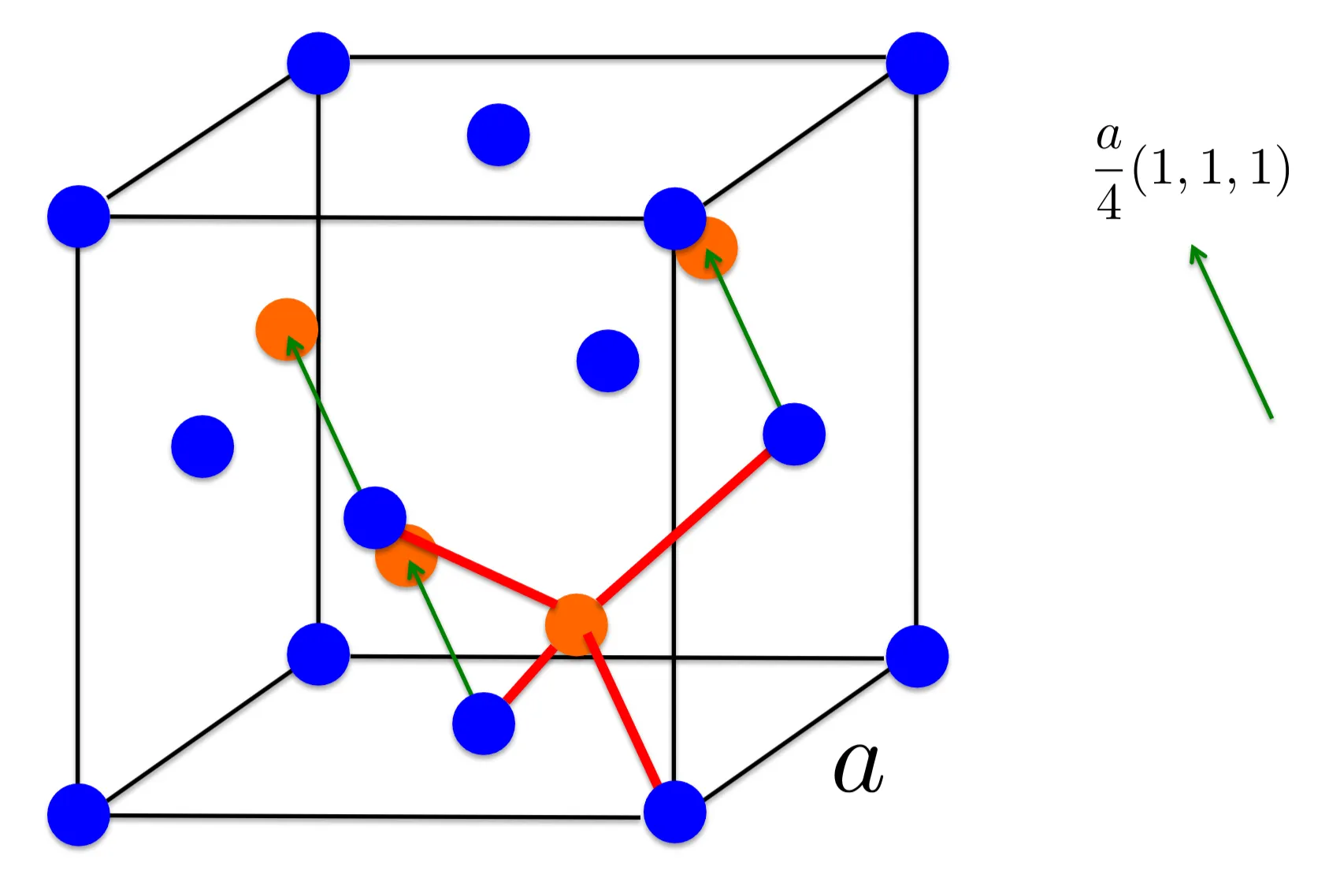
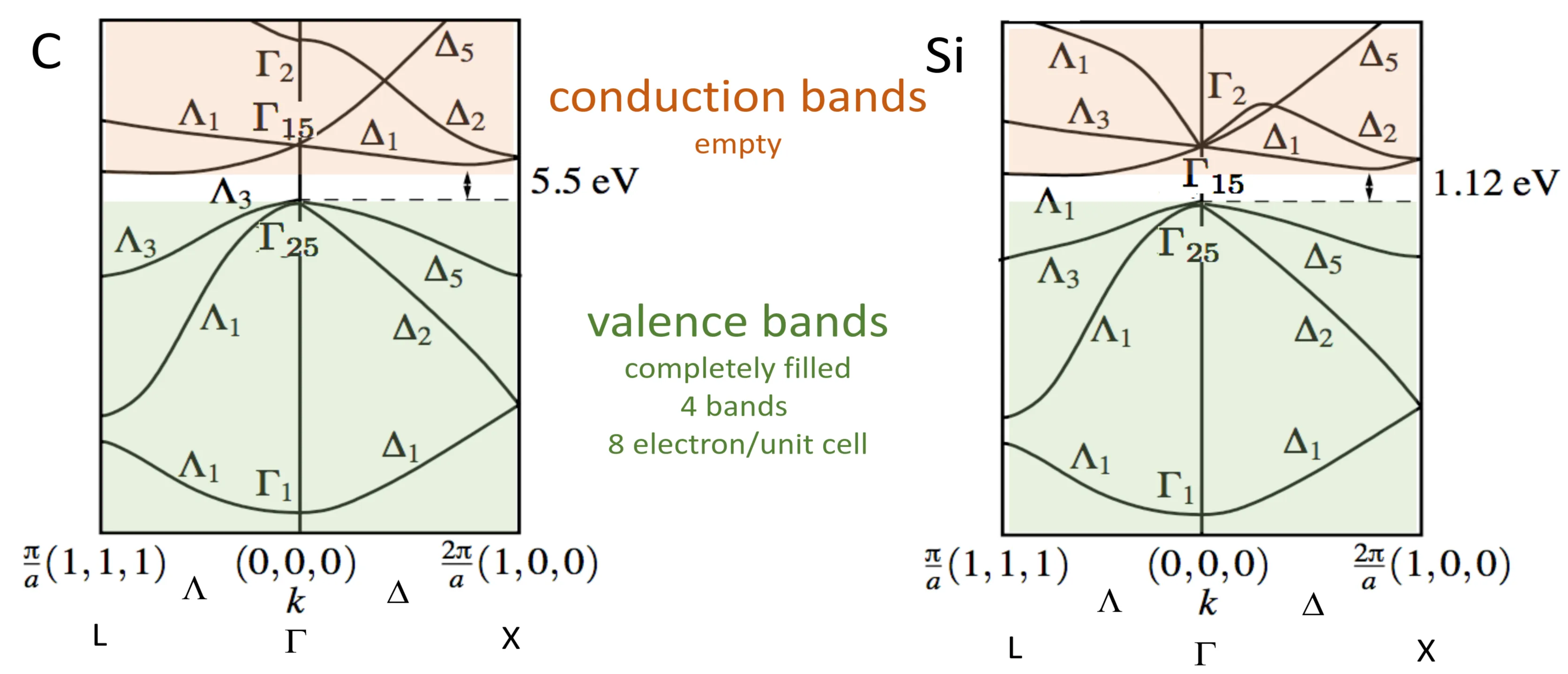
The most important semiconductor for technological applications is silicon (Si) that - like carbon (C), germanium (Ge) and tin (Sn) - belongs to the group IV of the periodic table. These elements have four electrons in their outermost shell in the configuration ( for C, for Si, for Ge, and for Sn). All four elements form crystals with a diamond structure, that is, a face-centred cubic lattice with a unit cell containing two atoms located at and (for Sn this is called ). The crystal structure is stabilised by hybridisation of the four valence electrons, leading to covalent bonding of oriented orbitals,
Locally, the nearest neighbours of each atom form a tetrahedron around it, which leads to the diamond structure of the lattice:
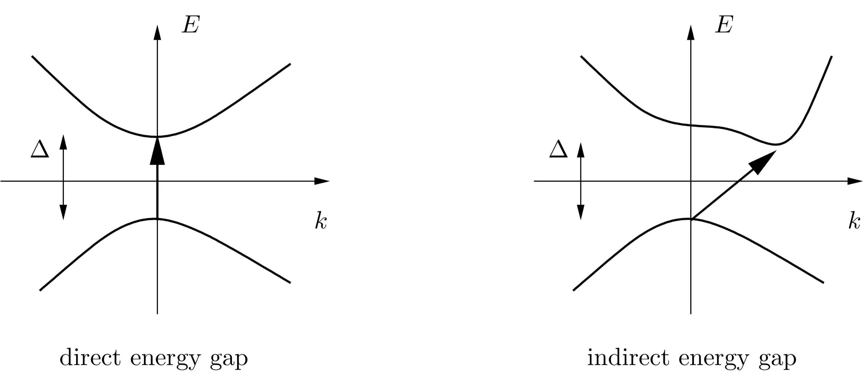
Let us look now at the electron count. The two atoms per unit cell provide together eight valence electrons per unit cell. With these we can fill four bands completely (see Section 1.6). Thus, in the ground state the lowest four bands constitute the completely filled valence bands, while all the upper ones are empty and represent conduction bands. The energy gap between the valence and conduction bands (top of valence band at and bottom of conduction bands at ) is smallest for a non-vanishing connecting -vector. We call this an indirect gap. This is the case for both C and Si. A typical example for a direct gap semiconductor is GaAs where the two sublattices of the crystal structure in diamond are occupied by an atom of the group III and V, respectively, in the periodic table.
Note that generally energy gaps in semiconductors and insulators are classified to be direct if the wave-vector connecting the maximum of the valence band and the minimum of the conduction band vanishes. Otherwise a gap is called indirect:
List of some facts about these materials of the group IV and compounds combining group III and V:
Carbon has an energy gap of around in the diamond structure. Thus, in this configuration it is not a semiconductor but an insulator. The large energy gap causes the transparency of diamond in the visible range (), as the electromagnetic energy in this range cannot be absorbed by the electrons.
The energy gap of silicon is and thus much smaller; furthermore, it is indirect.
Germanium has an indirect gap of .
GaAs and GaN have a direct energy gap of and , respectively.
2.2 Elementary Excitations in Semiconductors
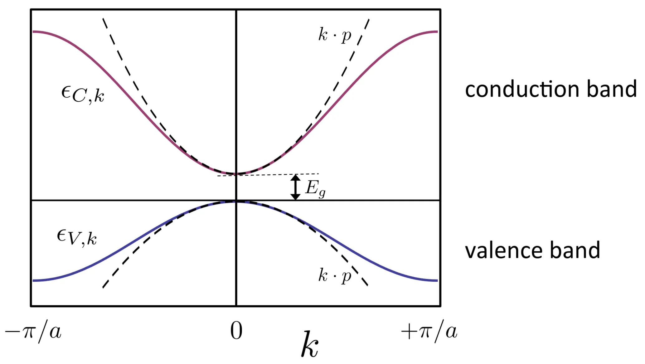
We consider a simple two-band model to illustrate the most basic properties of the excitation spectrum of a semiconductor. The Hamiltonian is given by
where and are the band energies of the valence band and conduction band, respectively. The figure shows the schematic band structure of a direct-gap semiconductor with a -approximation around the top of the valence and the bottom of the conduction band:
The operator creates (annihilates) an electron with (lattice) momentum and spin in the band . In the ground state ,
the valence band is completely filled, whereas the conduction band is empty. The product on the right-hand side runs over all wave vectors in the first Brillouin zone. The ground state energy is given by
The total momentum and spin of the ground state vanish. We next consider single electron excitations from that ground state.
Where is the chemical potential? We assume a simple band structure for a direct-gap semiconductor based on the approximation:
Now we calculate the electron distribution. The overall electron density is :
The density of electrons in the conduction and valence band for small finite temperature are given by
and
Here we assumed that both and are much larger than . Now we see that electron count gives such that we can set the two lines of the above equation equal to obtain for the chemical potential,
At the chemical potential is exactly in the centre of the band gap and then moves with increasing , if the effective masses are different. Note also that for small temperatures the thermally activated carriers, electrons and holes, are well described by the classical Maxwell-Boltzmann distribution, as was used in the approximation of the integrals.
2.2.1 Electron-Hole Excitations
A simple excitation of the system consists of removing an electron (that is, creating a hole) from the valence band and inserting it into the conduction band. We write such an excitation as
where we remove an electron with lattice momentum and spin in the valence band and replace it by an electron with and in the conduction band. The possibility of changing the spin from to and of shifting the wave vector of conduction electrons by is included.
Furthermore is assumed to be normalised. The electron-hole pair may either be in a spin-singlet (pure charge excitation ) or a spin-triplet state (spin excitation ). Apart from spin, the state is characterised by the wave vectors and .
To define the excitation energy: if we consider the eigenenergy of a state with an electron-hole excitation we obtain
which includes in also the ground state energy . Thus, with
we may combine these relations to obtain the excitation energy only, through the commutator. The excitation energy can be obtained by
such that,
The spectrum of the electron-hole excitations with fixed is determined by the spectral function
where is energy eigenstate of with energy . Since corresponds to an electron-hole excitation which is an eigenstate of only being such excitations will give a non-vanishing matrix element. Consequently, we find
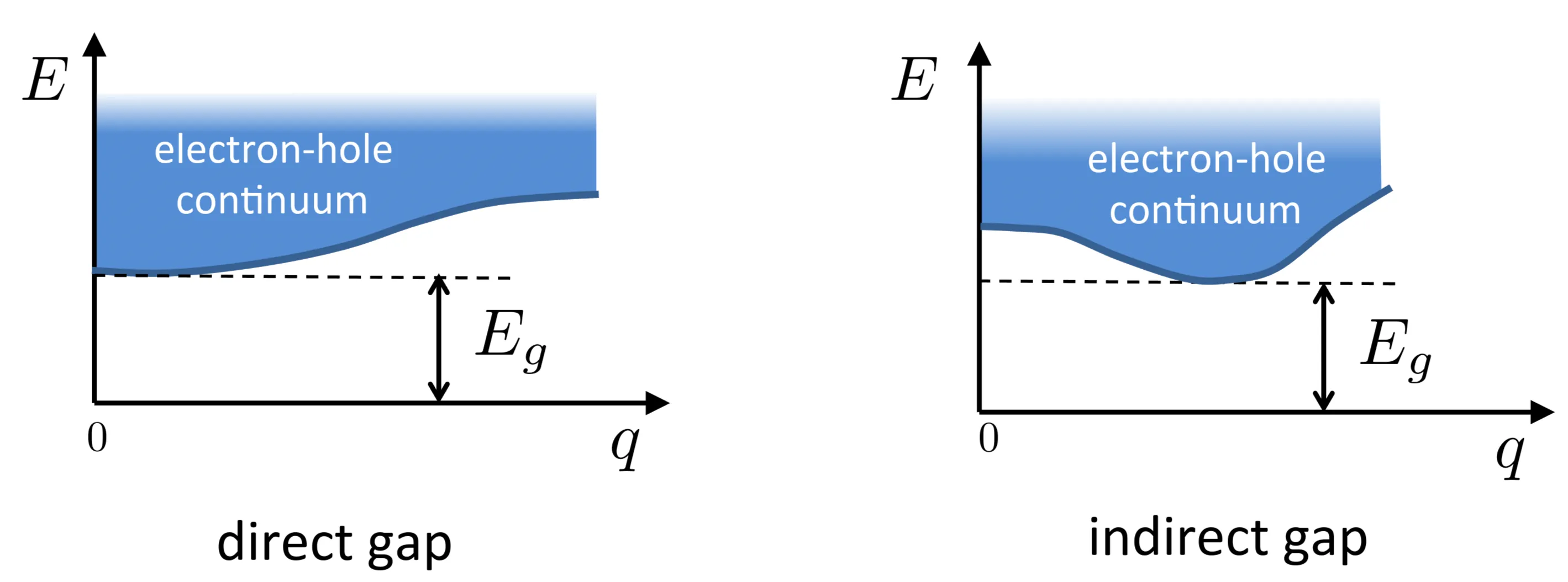
Excitations exist for all pairs and for which does not vanish, thus, only above a -dependent threshold, which is minimal for , where for a direct (indirect) energy gap. As is arbitrary, there is a continuum of excited states above the threshold for each (as illustrated in the conceptual depiction of excitation spectra). The magnitude of (not depicted here) is the density of excitations with (momentum , energy ). Note that the matrix elements are only exactly 1 if is an exact eigenstate of which is not true when we take electron-electron interactions into account as below.
For the electron-hole excitations considered here, interactions among them were assumed to be irrelevant, and the electrons involved are treated as non-interacting particles. Note the analogy with the Dirac-sea in relativistic quantum mechanics: The electron-hole excitations of a semiconductor correspond to electron-positron pair creation in the Dirac theory.
2.2.2 Excitons
Taking into account the Coulomb interaction between the electrons, there is another class of excitations called excitons. In order to discuss them, we extend the previously defined two-band Hamiltonian by the Coulomb interaction,
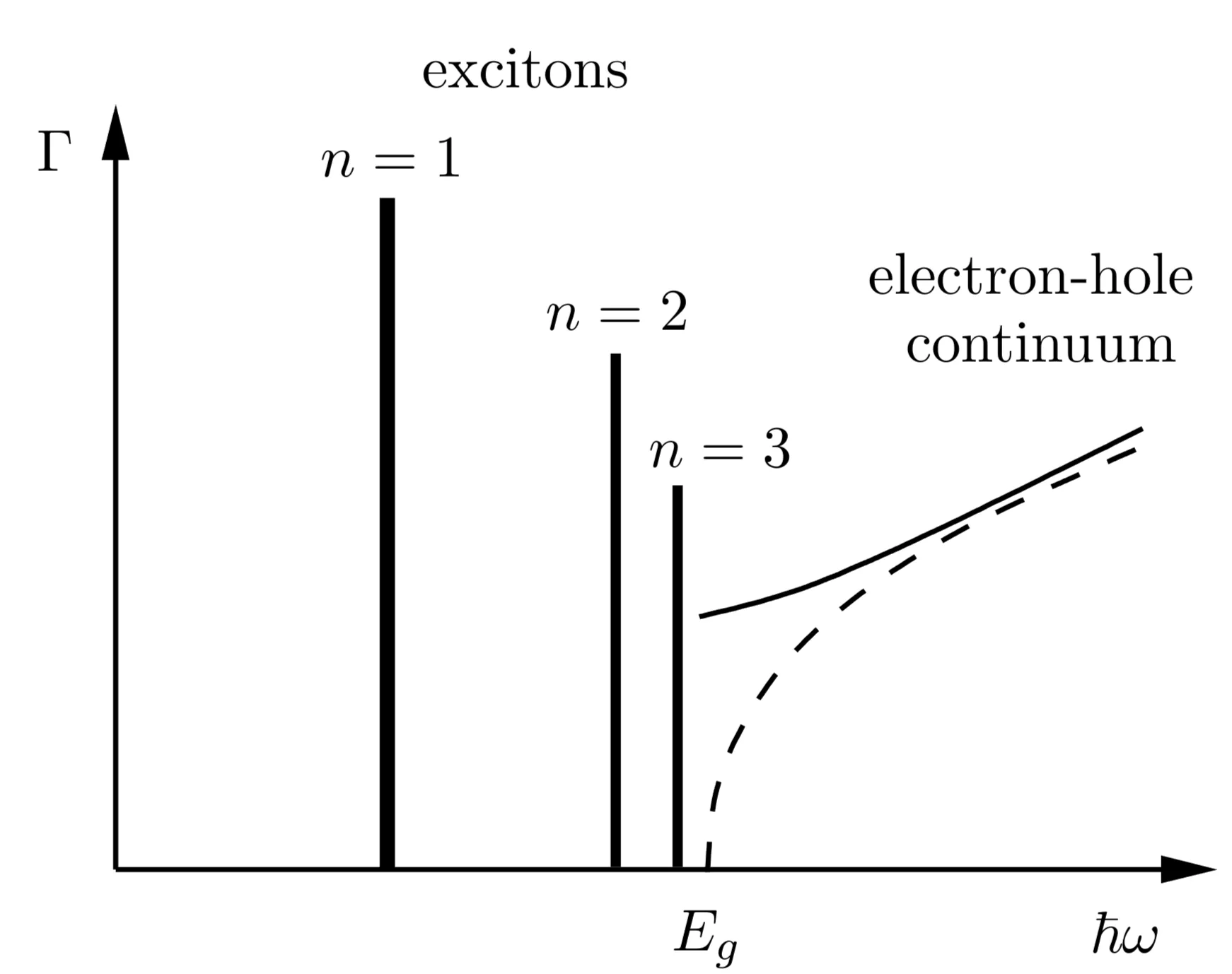
The figure shows the electron-hole excitation spectrum for direct and indirect gap semiconductors, excitation energy versus momentum transfer . Excitations exist in the shaded region, where .
where the field operators are defined by
where are the Bloch functions of the band . Now, we consider a general particle-hole state,
and demand that it satisfies the stationary Schrödinger equation . Note that compared to before, we introduce the momentum transfer in a "symmetrised" way. This two-body problem can be expressed as
The matrix elements are given by
and
The first term is the exchange term, and the second term the direct term of the Coulomb interaction. Now we consider a semiconductor with a direct energy gap at the -point and also focus on small momentum transfers . Thus, the most important wave vectors are those around . We approximate
which is reasonable for . In the same manner, we see that
Note that the semiconductor is a dielectric medium with a dielectric constant . Classical electrodynamics states that
that is, the Coulomb potential is partially screened due to dielectric polarisation. Including this effect in the Schrödinger equation phenomenologically, the matrix element for takes on the form
Thus, we can write the stationary Schrödinger equation derived earlier as
We include the band structure using the - approximation which, for a direct energy gap, leads to
For simplicity we assume now that . We define a so-called envelope function by
This function satisfies the differential equation
where is the reduced mass, that is, and total mass .
The stationary equation is equivalent to the Schrödinger equation of a hydrogen atom. The energy levels then are given by
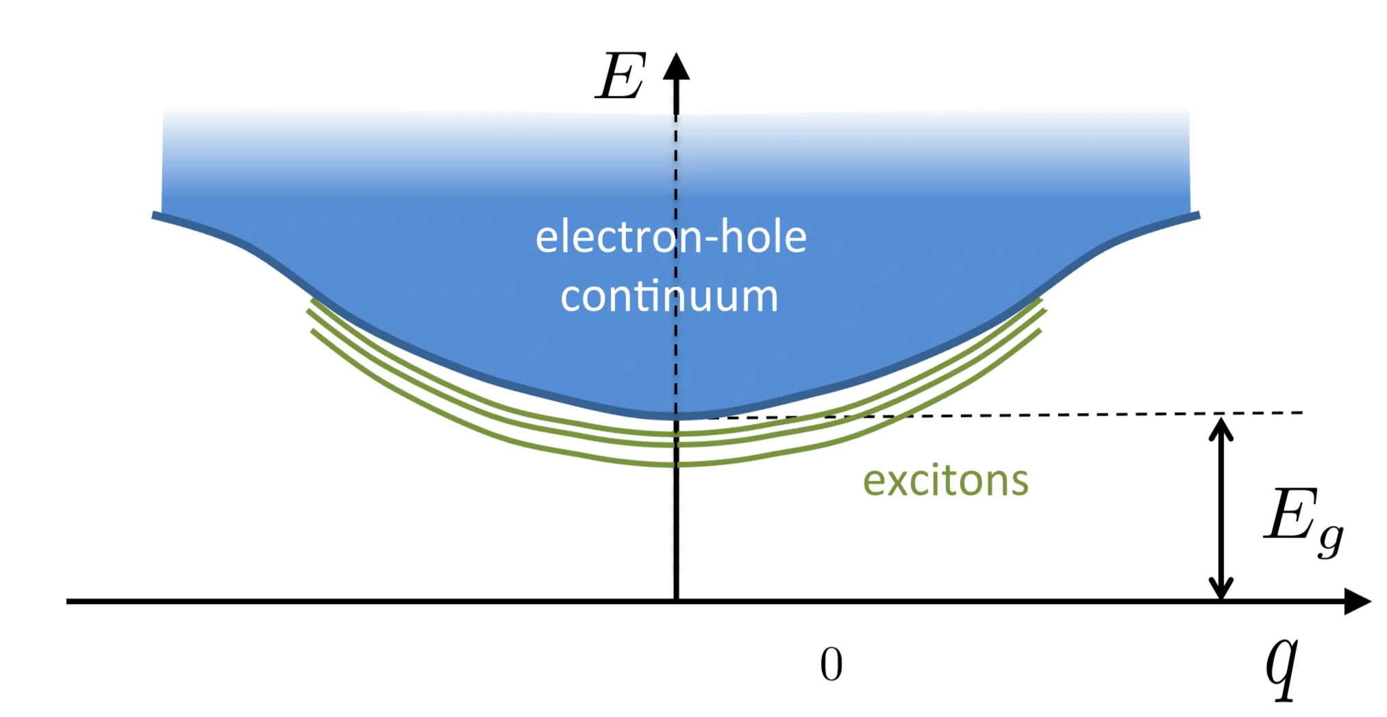
which implies that there are excitations below the particle-hole continuum, corresponding to particle-hole bound states. This excitation spectrum is discrete and there is a well-defined relation between energy and momentum , which is the wave vector corresponding to the centre of mass of the particle-hole pair. This non-trivial quasi-particle is called exciton. In the present approximation it takes on the form of a simple two-particle state. In fact, however, it may be viewed as a collective excitation, as the dielectric constant includes the polarisation by all electrons. When the screening is neglected, the excitonic states would not make sense as their energies would not be within the band gap but much below. For the case of weak binding considered above, the excitation is called a Wannier exciton. The typical binding energy is
Typical values of the constants on the right-hand side are and , so that the binding energy is in the meV range. This energy is much smaller than the energy gap, such that the excitons are inside the gap:
The exciton levels are dispersive and their spectrum becomes increasingly dense with increasing energy, similar to the hydrogen atom. When they merge with the particle-hole continuum the bound state is 'ionised', that is, the electron and the hole dissociate and behave like independent particles.
Strongly bound excitons are called Frenkel excitons. In the limit of strong binding, the pair is almost local, so that the excitation is restricted to a single atom rather than involving the whole semiconductor band structure.
Excitons are mobile, but they carry no charge, as they consist of an electron and a hole with opposite charges. Their spin quantum number depends on and . If the exciton is a spin singlet, while for it has spin triplet character, both corresponding to integer spin quasi-particles. For small densities they approximately obey Bose-Einstein statistics, as they are made from two Fermions. In special cases, Bose-Einstein condensation of excitons can be observed experimentally.
2.2.3 Optical Properties
Excitation in semiconductors can occur via the absorption of electromagnetic radiation. The energy and momentum transferred by a photon is and , respectively. With the linear light dispersion relation and the approximation , we can estimate this momentum transfer in a semiconductor
where denotes the speed of light, the lattice constant, and the fine structure constant. With this, the momentum transfer from a photon to the excited electron can be ignored. In other words, pure electromagnetic excitations lead only to 'direct' excitations. For semiconductors with a direct energy gap (for example, GaAs) the photo-induced electron-hole excitation is most easy and yields absorption rates with the characteristics
Here, the terms "dipole-allowed" and "dipole-forbidden" have a similar meaning as in the excitation of atoms regarding whether matrix elements of the type are finite or vanish, respectively. Obviously, dipole-allowed transitions occur at a higher rate for photon energies immediately above the energy gap , than for dipole-forbidden transitions.
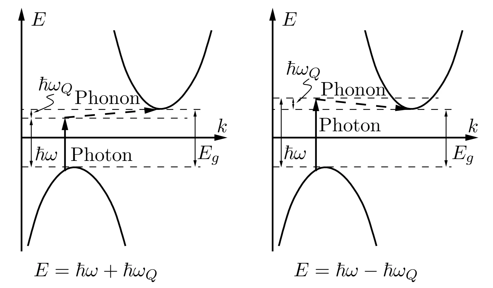
For semiconductors with indirect energy gap (for example, Si and Ge), the lowest energy transition connecting the top of the valence band to the bottom of the conduction band is not allowed without the help of phonons (lattice vibrations), which contribute little energy but much momentum transfer, as with and the sound velocity . The requirement of a phonon assisting in the transition reduces the transition rate to
where are constants and corresponds to the wave vector of the phonon connecting the top of the valence band and the bottom of the conduction band. There are two relevant processes: either the phonon is absorbed (-process) or it is emitted (-process). The next figure shows the phonon-assisted photon absorption in a semiconductor with indirect gap: phonon absorption (left panel) and phonon emission (right panel).
In addition to the absorption into the particle-hole spectrum, absorption processes inducing exciton states exist. They lead to discrete absorption peaks below the absorption continuum. This is the situation in a direct-gap semiconductor:
Naturally, the recombination of electrons and holes is important as well; in particular, if it is a radiative recombination, that is, leads to the emission of a photon. Additionally, other recombination channels such as recombination at impurities, interfaces and through Auger processes are possible. The radiative recombination for the direct-gap semiconductors is most relevant for applications. The photon emission rate follows the approximate law
with the photon density . This yields the dominant rate for very close to .
2.3 Doping Semiconductors
Let us replace a Si atom in a Si semiconductor by aluminium (Al) from group III or phosphorus (P) from group V, which then act as impurities in the crystal lattice. Both Al and P are in the same row of the periodic table. Aluminium has one valence electron less than Si, while phosphorus has one more. Their electron configurations are given by
2.3.1 Impurity State
We consider the case of a P-impurity contributing an additional electron whose dynamics is governed by the conduction band of the semiconductor. For simplicity, we describe the conduction band by a single isotropic band with effective mass ,
In the neutral Si background, the phosphorus (P) ion represents a positively charged centre, which attracts its additional electron. In the simplest model, this situation is described by the so-called Wannier equation
which is nothing else than the static Schrödinger equation for the hydrogen atom, where the dielectric constant measures the screening of the ionic potential by the surrounding electrons. Analogous to the discussion of the exciton states, is an envelope wave function of the electron. Therefore, the low energy states of the additional electron are bound states around the P ion. The electron may become mobile when this "reduced hydrogen atom" is ionised. The binding energy relative to the minimum of the conduction band given by
for and the effective radius (corresponding to the renormalised Bohr radius in the material) of the lowest bound state reads
where is the Bohr radius for the hydrogen atom. For Si we find and , such that
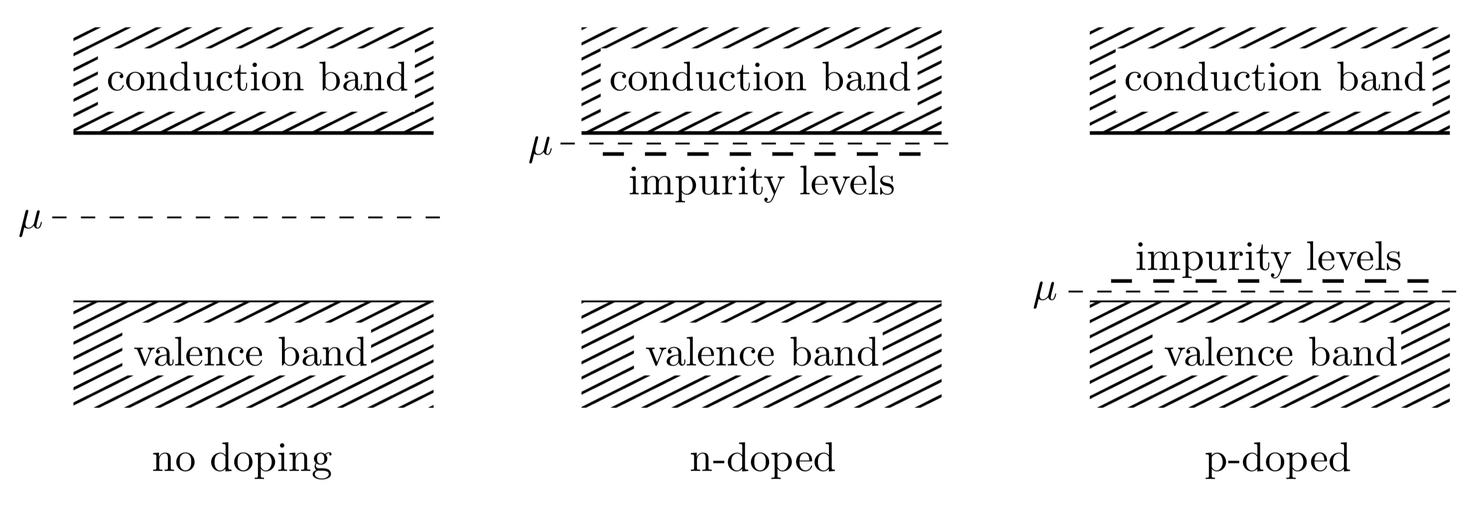
Thus, the resulting states are weakly bound, with energies inside the band gap. We conclude that the net effect of the P-impurities is to introduce additional electrons into the crystal, whose energies lie just below the conduction band ( while ). Therefore, they can easily be transferred to the conduction band by thermal excitation (ionisation). One speaks of an n-doped semiconductor (n: negative charge). In full analogy one can consider Al-impurities, thereby replacing electrons with holes: An Al-atom introduces an additional hole into the lattice which is weakly bound to the Al-ion (its energy is slightly above the band edge of the valence band) and may dissociate from the impurity by thermal excitation. This case is called p-doping (p: positive charge). In both cases, the chemical potential is tied to the dopant levels, that is, it lies between the dopant level and the valence band for p-doping and between the dopant level and the conduction band in case of n-doping:
The electric conductivity of semiconductors (in particular at room temperature) can be tuned strongly by doping with so-called donors (n-doping) and acceptors (p-doping). Practically all dopant atoms are ionised, with the electrons/holes becoming mobile. Combining differently doped semiconductors, the possibility to engineer electronic properties is enhanced even more. This is the basic reason for the semiconductors being ubiquitous in modern electronics.
2.3.2 Carrier Concentration
Let us briefly compare the carrier concentration in doped and undoped semiconductors at room temperature. Carriers are always created in form of electron-hole pairs, following the "reaction formula"
where denotes a photon which is absorbed (-creation) or emitted (-recombination) and accounts for the energy balance. The carrier concentration is described by a mass action law of the form,
where and are parameters specific to the semiconductor. In the case of undoped silicon at . Thus, for the undoped semiconductor we find . On the other hand, for n-doped Si with a typical donor concentration of we can assume that most of the donors are ionised at room temperature such that
and
We conclude, that in n-doped semiconductors the vast majority of mobile carriers are electrons, while the hole carriers are negligible. The opposite is true for p-doped Si.
2.4 Semiconductor Devices
Semiconductors are among the most important components of current high-technology. In this section, we consider a few basic examples of semiconductor devices.
2.4.1 pn-Contacts
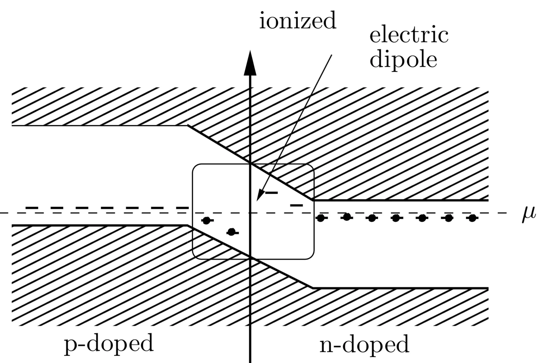
The so-called pn-junctions (made by bringing a p-doped and an n-doped version of the same semiconductor into contact) are used as rectifiers. When contacting the two types of doped semiconductors the chemical potential, which is pinned by the dopant (impurity) levels, determines the behaviour of the electrons at the interface. In electrostatic equilibrium, the chemical potential is constant across the interface. This is accompanied by a "band bending" leading to the ionisation of the impurity levels in the interface region, as depicted conceptually. Consequently, these ions produce an electric dipole layer which induces an electrostatic potential shift across the interface. Additionally, the carrier concentration is strongly reduced in the interface region (depletion layer).
In the absence of a voltage over the junction, the net current flow vanishes because the dipole is in electrostatic equilibrium. This can also be interpreted as the equilibrium of two oppositely directed currents, called the drift current and the diffusion current . From the point of view of the electrons, the dipole field exerts a force pulling the electrons from the p-side to the n-side. This leads to the drift current . On the other hand, the electron concentration gradient leads to the diffusion current from the n-side to the p-side. The diffusion current is directed against the potential gradient, so that the diffusing electrons have to overcome a potential step. The equilibrium condition for is given by
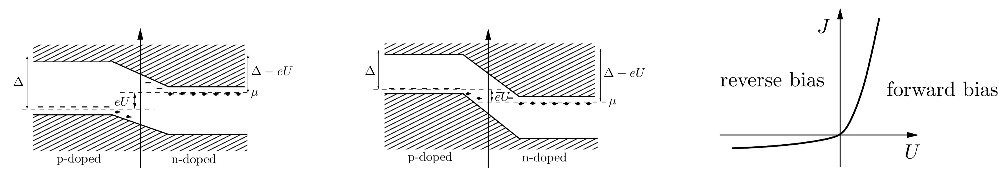
where . Both currents are essentially determined by the factor . For the drift current, the exponential behaviour stems from the dependence of the current on the concentration of mobile charge carriers (electrons and holes on the p-side and n-side, respectively), which are created by thermal excitation (Boltzmann factor). Applying a voltage does not change this contribution significantly. For the diffusion current however, the factor describes the thermal activation over the dipole barrier, which in turn strongly depends on the applied voltage . For zero voltage, the height of the barrier is essentially given by the energy gap . With an applied voltage, this is modified according to , where is the difference of the chemical potentials between the n-side and the p-side. From these considerations, the well-known current-voltage characteristic of the pn-junctions follows directly as
For , the current is rapidly enhanced with increasing voltage. This is called forward bias. By contrast, charge transport is suppressed for (reverse bias), leading to small currents only. The current-voltage characteristic shows a clearly asymmetric behaviour, which can be used to rectify ac-currents. Rectifiers (or diodes) are an important component of many integrated circuits.
2.4.2 Semiconductor Diodes
2.4.2.1 Light Emitting Diode
As mentioned above, the recombination of electrons and holes can lead to the emission of photons (radiative recombination) with a rather well-defined frequency essentially corresponding to the energy gap . An excess of electron-hole pairs can be produced in pn-diodes by running a current in forward direction. Using different semiconductors with different energy gaps allows to tune the colour of the emitted light. Direct-gap semiconductors are most suitable for this kind of devices. Well-known are the semiconductors of the GaAs-GaN series. These techniques are commonly used in LED (Light Emitting Diode) lamps.
There appear efficiency problems concerning the emission of light by semiconductors. In particular, the difference in refractive indices inside and outside the device leads to large reflective losses. Thus, the efficacy of diode light sources, defined as the number of photons emitted per created particle-hole pair, is small, but still larger than the efficiency of conventional dissipative light bulbs.
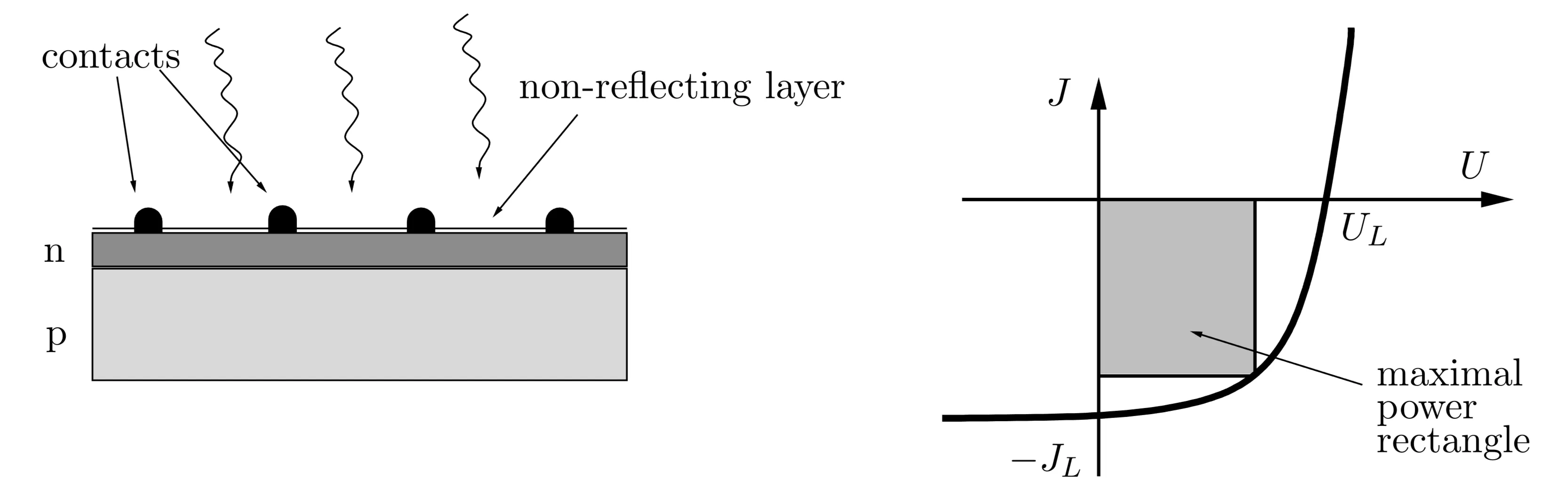
2.4.2.2 Solar Cell
Inversely to the previous consideration, the population of charge carriers can be changed by the absorption of light. Suppose that the n-side of a diode is exposed to irradiation by light, which leads to an excess of hole carriers (minority charge carriers). Some of these holes will diffuse towards the pn-interface and will be drawn to the p-side by the dipole field. In this way, they induce an additional current modifying the current-voltage characteristics to
It is important for the successful migration of the holes to the interface dipole that they do not recombine too quickly. When , the voltage drop across the diode is
The maximum efficiency is reached by applying an external voltage such that the product is maximised, where :
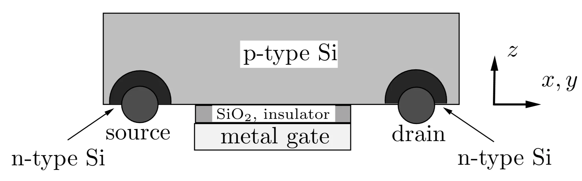
2.4.2.3 MOSFET
The arguably most important application of semiconductors is the transistor, an element existing with different architectures. Here we briefly introduce the MOSFET (Metal-Oxide-Semiconductor-Field-Effect-Transistor). A transistor is a switch allowing to control the current through the device by switching a small control voltage. In the MOSFET, this is achieved by changing the charge carrier concentration in a p-doped semiconductor using a metallic gate. The basic design of a MOSFET is as follows: A thin layer of is deposited on the surface of a p-type semiconductor. is a good insulator that is compatible with the lattice structure of Si. Next, a metallic layer, used as a gate electrode, is deposited on top of the insulating layer.
The voltage between the Si semiconductor and the metal electrode is called gate voltage . The insulating layer ensures that no currents flow between the electrode and the semiconductor when a gate voltage is applied. The switchable currents in the MOSFET flow between the source and the drain which are heavily n-doped semiconductor regions. Depending on the applied gate voltage three different regimes can be realised:
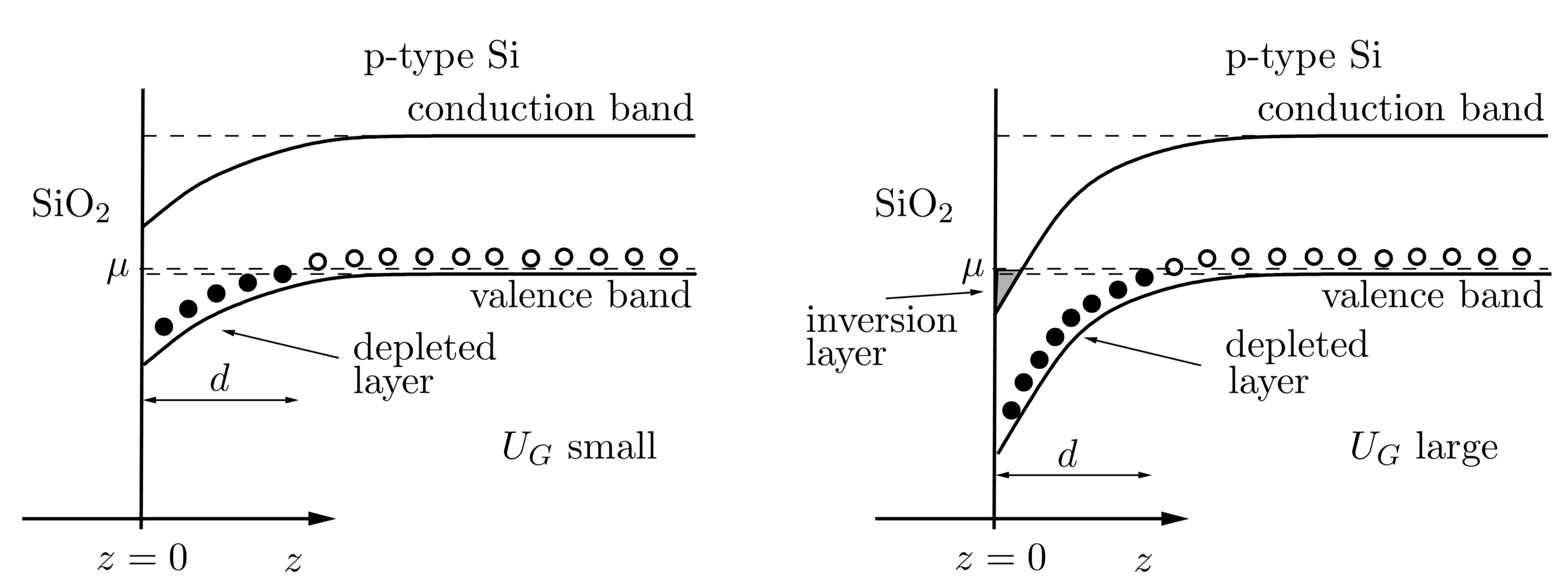
Essentially no current flows, as the conduction band of the p-doped semiconductor is empty. The doping states (acceptor levels) are occupied by thermal excitations.
In this case, the energy of the Si bands is lowered, such that in a narrow region within the p-doped Si the acceptor levels drops below the chemical potential and the states are filled with electrons (or, equivalently, holes are removed). This depletion layer has the extension measured from the interface. The negative charge of the acceptors leads to a position-dependent potential , where is the distance from the boundary between and Si. This potential satisfies the simple one-dimensional Poisson equation
where the charge density originates in the occupied acceptor levels,
and is the density of acceptors. The boundary conditions are given by
The solution for then reads
The thickness of the depletion layer increases with increasing gate voltage .
When the applied gate voltage is sufficiently large, a so-called inversion layer is created:
Close to the boundary, the conduction band is bent down so that its lower edge lies below the chemical potential. The electrons accumulating in this inversion layer providing carriers connecting the n-type source and drain electrodes and producing a large, nearly metallic, current between source and drain. Conduction band electrons accumulating in the inversion layer behave like a two-dimensional electron gas. In such a system, the quantum Hall effect (QHE), which is characterised by highly unusual charge transport properties in the presence of a large magnetic field, can occur.